
Solar Energy, Solar Energy Basics
by Federica Rustico 3 years ago 15 min
The advent of solar energy has introduced a green, sustainable solution for our growing energy needs. Solar panels, the fundamental components of any solar energy system, harness the power of the sun to produce electricity. But how are these technologically advanced devices made? In this article, we’ll delve into the complex solar panel manufacturing process.
Solar panel manufacturing is a complex, multi-step process, involving a range of scientific disciplines and high precision procedures to turn raw materials into energy-generating devices. Let’s analyze each step of the production process.
Creating a solar panel begins with the careful procurement and preparation of the essential raw materials. Foremost among these materials is silicon, generously available in the form of silica in sand. However, the transformation of silica into a form suitable for solar panel production is an intricate and high-precision process. To begin, the silica is subjected to intense heating in the presence of carbon within an electric arc furnace. This interaction results in the formation of metallurgical-grade silicon, a significantly purified form compared to the raw silica. However, for solar panel production, an even higher degree of purity is needed.
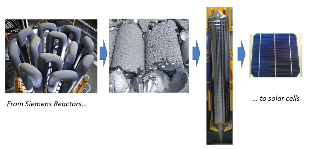
To achieve this, the metallurgical-grade silicon is put through a series of complex chemical reactions in what is often referred to as the Siemens process. In this process, the silicon is converted into a volatile compound, typically trichlorosilane, by reacting with hydrogen and a silicon-carrying catalyst. This compound is then distilled to increase its purity before being deposited onto a thin rod of silicon in a high-temperature reactor. The result of this deposition is ultra-pure, semiconductor-grade silicon – the foundational material for the production of solar cells.
The purity of silicon in solar cells is essential due to the way semiconductors work. Semiconductors are materials that have an electrical conductivity between that of conductors (like copper and gold) and insulators (like rubber and glass). Silicon is one of the most common semiconductors used in electronics and solar cells. A semiconductor’s behavior is due to its atomic structure and how its electrons react to energy, such as sunlight in the case of solar panels. Pure silicon has a precise crystalline structure. When energy from the sun hits a solar cell, it gives the silicon’s electrons enough energy to move around. These movements create an electric current, which we can then use as electricity.
If the silicon is impure, its atomic structure might be interrupted by atoms of other elements. This interruption can hinder the movement of the electrons, reducing the efficiency of the solar cell in converting sunlight into electricity. In other words, the purer the silicon, the better it can conduct electricity when exposed to sunlight, leading to more efficient solar panels. The purity requirement varies among the three types of solar cells: monocrystalline, polycrystalline, and thin-film.
Monocrystalline Solar Cells
These are made from a single, pure crystal structure. This single structure allows electrons to move more freely, resulting in a higher efficiency. However, creating such a pure crystal structure is expensive, which makes monocrystalline solar cells more costly than other types.
Polycrystalline Solar Cells
These are created from multiple crystal structures, which makes them less pure than monocrystalline cells. This impurity can impede the flow of electrons, resulting in lower efficiency. However, the process of making polycrystalline cells is simpler and cheaper, making these cells more affordable.
Thin-Film Solar Cells
These cells are created by depositing a thin layer of semiconductor material (like silicon, cadmium telluride, or copper indium gallium selenide) onto a substrate. The semiconductor layer in thin-film cells is typically less pure than in other types of cells. As a result, thin-film cells are less efficient than monocrystalline or polycrystalline cells. However, they are easier and cheaper to produce, and they perform better in low-light conditions and high temperatures.
So, in a nutshell, the purity of silicon matters because it directly affects the efficiency of solar panels in converting sunlight into electricity. But there’s a trade-off: achieving higher purity comes with a higher manufacturing cost. Therefore, different types of solar panels balance this trade-off in different ways, resulting in varying levels of efficiency, cost, and other characteristics.
Once the ultra-pure silicon has been produced, the next task is to convert it into a form that can be easily worked with to manufacture solar cells. This step involves the crystallization of the silicon and is a marvel of material science. The prevalent method for achieving this is the Czochralski process. In this technique, a small piece of high-purity, crystalline silicon, known as a seed crystal, is dipped into a crucible containing molten silicon. The temperature of the crucible is carefully controlled to maintain the silicon just above its melting point.
As the seed crystal is slowly lifted and rotated, the molten silicon solidifies onto it, matching the crystal structure of the seed. This is a delicate process, with the rate of lifting and rotation needing to be precisely controlled to prevent the formation of multiple crystal structures. If performed correctly, the end result is a large, cylindrical crystal of silicon, often referred to as a silicon boule. This boule, typically measuring several inches in diameter, is a single crystal of silicon, making it ideal for the subsequent manufacturing steps. Its single-crystal nature minimizes electronic defects, thus enhancing the efficiency of the eventual solar cells. In sum, these two critical stages of the solar panel manufacturing process showcase a blend of chemical engineering and material science. They serve as the bedrock upon which the rest of the solar panel production process is built, underlining the need for careful control and high precision.
After the successful crystallization of silicon, the silicon boule (aka the large, single-crystal silicon cylinder) must then be meticulously crafted into thin, disc-shaped slices, known as wafers. This procedure requires a high degree of precision and delicacy to ensure that each wafer is cut uniformly without damage to the material structure. The boule is mounted on a sophisticated cutting machine, where a diamond-tipped, multi-wire saw is used to slice it. The wafers produced are approximately 200 micrometers thick – roughly twice the thickness of a standard piece of paper. This thickness strikes a balance between maintaining structural integrity and allowing light to penetrate the material.
Following slicing, the wafers undergo a rigorous polishing process. This polishing eliminates any surface irregularities and damage caused by the slicing process, providing a clean, smooth base for the subsequent processing steps. The polishing process can involve chemical mechanical polishing, a procedure that uses a combination of chemical reactions and mechanical force to achieve a flawless surface.
With a polished silicon wafer at hand, it’s time to transform it into a functioning solar cell capable of converting sunlight into electricity. This transformation involves several carefully controlled processes that alter the electrical properties of the silicon and prepare it to absorb sunlight effectively. The first step in this transformation is the creation of a p-n junction within the silicon wafer. This junction is formed by a process called doping, where specific impurities are deliberately introduced into the silicon. Typically, the wafer is initially doped with boron (a type III element) to create a p-type silicon layer. The wafer is then subjected to a high-temperature diffusion process with phosphorus (a type V element), forming a thin layer of n-type silicon on the surface. The area where the p-type and n-type regions meet forms the p-n junction, a one-way barrier for electrical current.
Subsequently, the wafer is coated with an anti-reflective layer, usually made of silicon nitride or silicon oxide. The purpose of this layer is twofold: first, to maximize the absorption of sunlight by reducing reflection, and second, to provide a protective layer against weather and other potential damage. This layer is applied using a technique such as plasma-enhanced chemical vapor deposition, which allows for a thin, uniform coating. These steps turn a simple silicon wafer into a solar cell capable of converting sunlight into electricity. Yet, there’s still more work to be done before it becomes a solar panel ready to harness the power of the sun. The detailed precision of each process underscores the intricate science and engineering at play in the creation of solar technology.
Once individual solar cells are fabricated, the task of assembly begins. This process involves aligning the cells into a desired configuration, which is typically a series arrangement. Series arrangement enables the cells to produce a higher voltage, making the panel more efficient. First, tabbing wires, which are thin ribbons of conductive material, are soldered onto the solar cells. These wires are crucial as they serve to connect all the cells together, allowing for the flow of electricity through them. An automated machine lays out the tabbing wires precisely onto the front surface of each cell, after which the cells are flipped and soldered in a string.
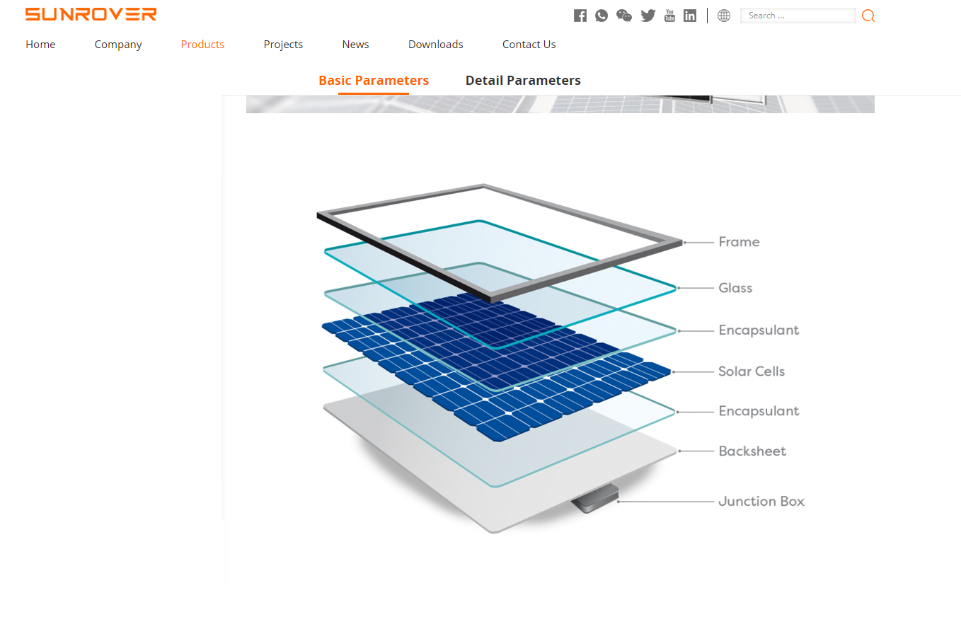
Once a string of solar cells is completed, these strings are then laid out onto a backing sheet, usually made of a durable, insulating material. The backing sheet acts as a supportive base for the cell strings. The positioning of the strings must be precise, as this arrangement dictates the electrical output and physical dimensions of the solar panel. Next, a layer of encapsulant material is spread on top of the cell strings, acting as an adhesive to bind the layers together. This encapsulant also provides electrical insulation and protection against environmental factors. Finally, a glass casing, typically made of tempered glass for its strength and transparency, is placed on top of the encapsulant layer. The glass casing’s primary function is to protect the cells while allowing sunlight to pass through. After being sealed, an aluminum frame is often added to provide further structural support to the panel.
After assembly, the solar panels undergo meticulous inspection and testing. The goal of these procedures is to guarantee that the panels are defect-free and perform to their expected efficiency levels. Initial inspections usually involve a visual check for any visible defects such as micro-cracks, soldering flaws, or alignment issues. This step can be performed manually by trained inspectors or with automated systems that utilize high-resolution imaging.
Once visual inspection is completed, the panels undergo a series of performance tests. A common test is the flash test, which simulates sunlight and measures the electrical output of the panel to confirm it aligns with expected values. The test uses a solar simulator that shines a light with an intensity and spectrum similar to the sun onto the panel. The electrical output, including voltage, current, and power, are then recorded. In addition, panels may be subjected to a thermographic inspection. In this procedure, an infrared camera scans the panels to identify any hot spots that could indicate potential faults or defects. This type of inspection is particularly useful as it can reveal issues not visible to the naked eye.
Finally, the panels may be put through durability testing, including stress tests like high-temperature, humidity, and mechanical load tests. These tests ensure the panel can withstand various weather conditions and long-term use. By the end of the inspection and testing phase, each solar panel should be ready to produce reliable, clean energy. The level of care and scrutiny in these stages exemplifies the commitment to quality and efficiency in the solar industry. This ensures that when a solar panel reaches a home, business, or utility site, it’s ready to perform optimally for many years to come.
Over the last ten years, the global production of solar photovoltaic (PV) panels has steadily moved from Europe, Japan, and the United States to China. The Asian nation’s over USD 50 billion investment in new PV supply capacity has spurred this transition, generating more than 300,000 jobs across the solar PV manufacturing spectrum since 2011. Currently, China’s control in the comprehensive manufacturing process of solar panels—spanning from polysilicon and ingots to wafers, cells, and modules—exceeds 80%.
Solar panels are created using different technologies, namely monocrystalline, polycrystalline, and thin-film. Monocrystalline panels, known for their efficiency and sleek appearance, are made from a single crystal structure. Despite the energy-intensive production process due to the high-temperature extraction of pure silicon, their efficiency and long lifespan somewhat balance out their initial environmental impact. On the other hand, polycrystalline panels are composed of multiple silicon crystals. These blue-colored panels are less energy-consuming to produce due to their more straightforward production process. However, their lower efficiency and shorter lifespan compared to monocrystalline panels could lead to a larger environmental footprint over time as replacements might be required more frequently. Finally, thin-film panels involve depositing one or more layers of photovoltaic material onto a substrate. While their production process is less energy-intensive and they use fewer raw materials than crystalline silicon panels, they tend to be less efficient and have shorter lifespans. This could potentially result in higher waste generation, plus certain types like CdTe panels contain cadmium, a toxic heavy metal that can pose environmental hazards if not managed properly at the end of the panel’s life.
Regardless of the production method, solar PV manufacturing, largely powered by fossil fuels, produces carbon emissions. However, considering the average solar panel’s lifespan of 25-30 years, solar panels only need to operate from 4 months to 4 years to offset their manufacturing emissions. This makes solar power a significant means of reducing overall carbon emissions in the long run. Since 2011, continuous innovation, primarily led by China, has halved the emissions intensity of solar PV manufacturing. Though absolute CO2 emissions from solar PV manufacturing have increased due to the expanding production in China, in 2021, it accounted for a mere 0.15% of energy-related global CO2 emissions. As power systems worldwide continue to transition towards decarbonization, we can expect the carbon footprint of PV manufacturing to decrease correspondingly.
Consequently, when evaluating the environmental impact of solar panels, it’s crucial to consider the balance between production, efficiency, lifespan, and end-of-life management. The solar industry is consistently trending towards greater efficiency and sustainability, with ongoing research and development seeking to minimize the environmental impact of solar panel production while maximizing panel efficiency.
China’s strategic focus on solar PV as a crucial sector and efforts to foster domestic demand have stimulated economies of scale and bolstered continuous innovation throughout the supply chain. This has contributed to an over 80% cost decline, making solar PV the most affordable electricity generation technology in many parts of the world. Furthermore, China’s solar PV exports were valued over USD 30 billion in 2021, nearly 7% of China’s trade surplus over the last five years.
The concentration of production in China – mainly in provinces like Xinjiang and Jiangsu where coal comprises more than 75% of the annual power supply – is a significant factor behind the fact that over 60% of the electricity used for global solar PV manufacturing is generated by coal. This scenario is primarily due to favourable government tariffs. However, the level of geographical concentration in global supply chains also presents potential challenges that governments need to confront. On a global scale, production of polysilicon, the key material for solar PV, is currently a bottleneck in an otherwise oversupplied supply chain, leading to tight global supplies and a quadrupling of polysilicon prices over the last year.
Chinese investments in Malaysia and Vietnam have also transformed these countries into significant exporters of PV products, contributing to around 10% and 5% respectively of their trade surpluses since 2017. The total value of global PV-related trade – including polysilicon, wafers, cells, and modules – exceeded USD 40 billion in 2021, a surge of over 70% from 2020. In conclusion, the solar panel manufacturing landscape is a complex global network shaped by various factors, including policy decisions, market trends, and technological advancements. The continued development and adoption of solar energy technologies hinge on addressing these interrelated challenges and optimizing the global supply chain.
The world of solar photovoltaic (PV) manufacturing has witnessed significant transformations over the past decade, with China emerging as a dominant player. As we examine the different types of solar panels – monocrystalline, polycrystalline, and thin-film – it’s evident that each has its unique manufacturing process, efficiency, lifespan, and environmental footprint. Despite the inherent carbon emissions during production, the operational lifespan of these panels provides a potent tool for offsetting these initial impacts, reinforcing solar power as an effective strategy in the global bid to reduce carbon emissions.
Moreover, the innovative strides being made in the solar industry, led primarily by China, demonstrate a promising trend towards sustainability and efficiency. Efforts are ongoing to reduce the environmental impact of solar panel production and to increase the efficiency of the panels themselves, creating a more sustainable future. The industry’s growth, despite its challenges, remains a testament to the power of human innovation and our collective commitment to transitioning towards a more sustainable and carbon-neutral future.
Purer silicon allows for better conductivity when exposed to sunlight, leading to more efficient solar panels.
They differ in their crystal structure, purity of silicon, manufacturing process, cost, and efficiency in converting sunlight into electricity.
Stay a while and read more posts like this

Bisera Apostolova 1 year ago
In recent years, Europe has witnessed a remarkable surge in the adoption of solar panels, marking a pivotal shift towards renewable energy. Data from the...
Renewable Energy, Solar Energy, Solar Energy Basics, Solar Technology
Kristina 1 year ago
“Unlock the Truth: Get the Facts on Solar Energy!” Introduction Solar energy is becoming increasingly popular as a renewable energy source, but there are...

Bisera Apostolova 1 year ago
Imagine a world where you’re able to cut your monthly energy expenditure substantially. A reality where your home isn’t reliant on finite,...